|
ADI公司的AD5780是18位電壓輸出數模轉換器(DAC),工作電壓為雙極電源,高達33V,正基準電壓為5V到VDD-2.5V,負基準電壓為VSS+2.5V到0V, 0°C到+125℃工作溫度,低噪音為8 nV/√Hz,增益誤差溫度系數為±0.018 ppm/℃,主要用在醫療儀器,測試和測量,工業控制,科學和航空儀表,數據采集系統,數字增益和失調調整以及電源控制.本文介紹了AD5780主要特性和產品亮點, 方框圖和典型應用電路,以及評估板EVAL-AD5780主要特性,方框圖,電路圖,材料清單和PCB布局圖. The AD5780 is a true 18-bit, unbuffered voltage output DAC that operates from a bipolar supply of up to 33 V. The AD5780 accepts a positive reference input range of 5 V to VDD − 2.5 V and a negative reference input range of VSS + 2.5 V to 0 V. Both reference inputs are buffered on chip and external buffers are not required. The AD5780 offers a relative accuracy specification of ±1 LSB maximum range, and operation is guaranteed monotonic with a ±1 LSB DNL maximum range specification. The part uses a versatile 3-wire serial interface that operates at clock rates of up to 35 MHz and is compatible with standard SPI, QSPI™ MICROWIRE™ and DSP interface standards. The part incorporates a power-on reset circuit that ensures that the DAC output powers up to 0 V in a known output impedance state and remains in this state until a valid write to the device takes place. The part provides an output clamp feature that places the output in a defined load state. AD5780產品亮點: True 18-bit accuracy. Wide power supply range of up to ±16.5 V. −0℃ to +125℃ operating temperature range. Low 8 nV/√Hz noise. Low ±0.018 ppm/℃ gain error temperature coefficient. AD5780主要特性: True 18-bit voltage output DAC, ±1 LSB INL 8 nV/√Hz output noise spectral density 0.025 LSB long-term linearity error stability ±0.018 ppm/℃ gain error temperature coefficient 2.5 μs output voltage settling time 3.5 nV-sec midscale glitch impulse Integrated precision reference buffers Operating temperature range: −0℃ to +125℃ 4 mm × 5 mm LFCSP package Wide power supply range of up to ±16.5 V 35 MHz Schmitt triggered digital interface 1.8 V-compatible digital interface AD5780應用: Medical instrumentation Test and measurement Industrial control Scientific and aerospace instrumentation Data acquisition systems Digital gain and offset adjustment Power supply control 
圖1.AD5780方框圖
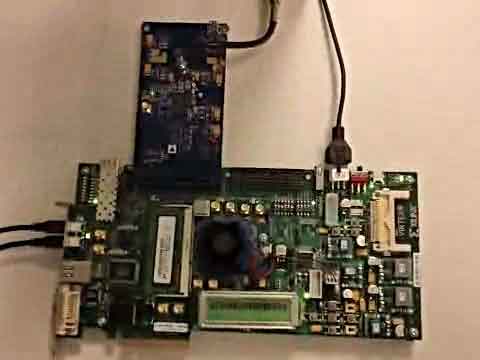
圖2.AD5780典型應用電路圖 評估板EVAL-AD5780 The EVAL-AD5780 is a full-featured evaluation board, designed to allow the user to easily evaluate all features of the AD5780 voltage output, 18-bit digital-to-analog converter (DAC). The AD5780 pins are accessible at on-board connectors for external connection. The board can be controlled by two means: via the on-board connector (J3), or via the system development platform connector (J4). The SDP board allows the evaluation board to be controlled through the USB port of a Windows® XP- (SP2 or later) or Vista-based (32-bit) PC using the AD5780 evaluation software.
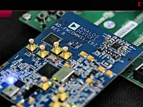
圖3.評估板EVAL-AD5780外形圖 評估板EVAL-AD5780主要特性: Full-featured evaluation board for the AD5780 Link options PC control in conjunction with Analog Devices, Inc., system development platform PC software for control
圖4.評估板EVAL-AD5780功能方框圖
圖5.評估板EVAL-AD5780電路圖(1)
圖6.評估板EVAL-AD5780電路圖(2)
圖7.評估板EVAL-AD5780電路圖:SDP板連接器 評估板EVAL-AD5780材料清單(BOM):
圖8.評估板EVAL-AD5780 PCB元件布局圖
圖9.評估板EVAL-AD5780 PCB頂層布局圖 詳情請見:  AD5780.pdf
(593.4 KB)
UG-256.pdf
(819.83 KB)
AD5780.pdf
(593.4 KB)
UG-256.pdf
(819.83 KB)
來源:網絡 |